
An RF or microwave LTCC grade should not be selected from one dielectric-constant value alone · The test frequency and method, dielectric loss, fired thickness, dimensional shrinkage, conductor system and actual circuit geometry all affect the evaluation
HTK’s approved LTCC page lists confirmed grades and representative source values for preliminary screening · The current controlled TDS and project sample remain the basis for qualification
1 Define the electrical requirement at the operating frequency
Always compare values measured at a relevant frequency and by a stated method · Data reported at 1 MHz and 10 GHz are not automatically interchangeable
- Target dielectric constant and acceptable tolerance
- Maximum dielectric loss or loss tangent
- Operating frequency range and bandwidth
- Impedance, resonator, antenna or filter requirement
- Temperature and environmental range used for evaluation
2 Translate green-sheet data into fired geometry
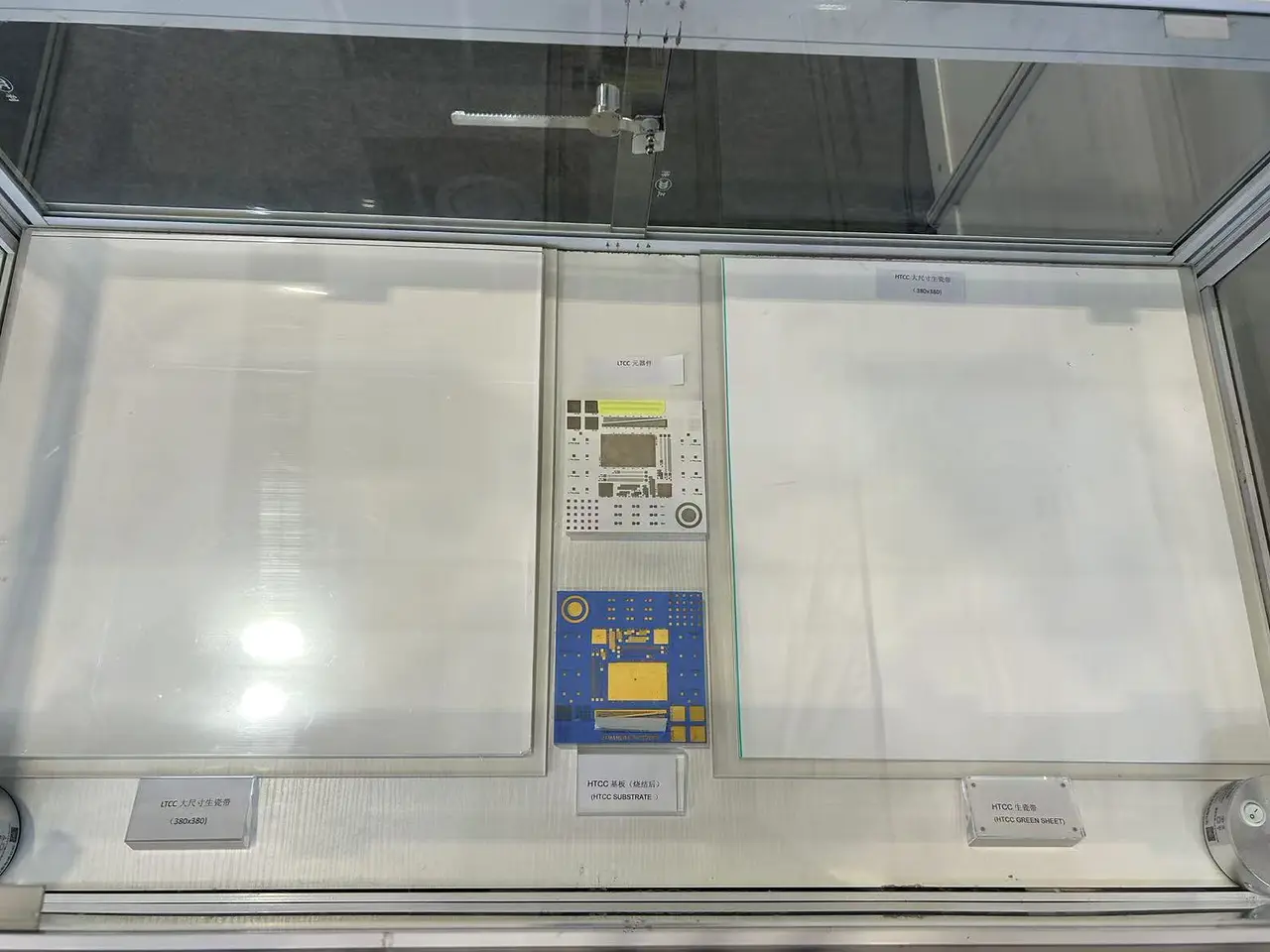
HTK’s current approved range identifies green-sheet thicknesses of 55–200 µm and a catalog format up to □500 mm for applicable grades · Actual availability and usable area require grade and project confirmation
- Green-sheet thickness and expected fired thickness
- XY shrinkage, Z shrinkage and allowed variation
- Sheet dimensions, usable area and registration strategy
- Layer count, cavities, vias and conductor thickness
- Finished substrate dimensions and tolerances
3 Review firing and conductor compatibility as one system
A conductor or paste that performs in one ceramic system is not automatically compatible with another · Confirm the matched material set and process window before circuit-level testing
- Peak temperature, dwell, ramp and cooling profile
- Firing atmosphere and furnace constraints
- Inner conductor, outer conductor and via-fill paste
- Co-fire or post-fire sequence
- Interaction between paste, ceramic, vias and printed geometry
4 Include mechanical and processing checks
- Handling strength and lamination behavior
- Via punching or laser process and fill quality
- Printing resolution and registration
- Warpage, flatness and surface condition after firing
- Dicing, metallization, assembly and inspection requirements
Suggested sample evaluation sequence
| Stage | Evaluation | Decision output |
|---|---|---|
| Screening | TDS, frequency-specific dielectric data, sheet format and process fit | Shortlist of candidate grades |
| Material coupon | Shrinkage, thickness, firing response and conductor interaction | Baseline process window |
| Test pattern | Lines, vias, registration, impedance or resonator response | Design and process corrections |
| Representative build | Actual layer stack and application geometry | Project qualification decision |